Looking inside the Sykes-Pickavant ACR
Published: 2014-05-17
The Sykes-Pickavant ACR is an automotive fault code reader and diagnostic tool. It's one of a small number of tools that can interface with early versions of the Modular Engine Management System (MEMS) that was used in Rover products in the 1990s. Sykes-Pickavant also produced later revisions of the ACR, which were named "ACR2" and "ACR4" and are distinguished by their blue plastic housings and, in the case of the ACR4, its larger LCD display. My experience with this tool is limited to the original revision (part number 300550 with the gray plastic housing) and I've only used it to communicate with a MEMS 1.6 SPi engine management system.
The ACR is actually able to interface with many different engine management systems by changing the removable "pod" and interface cable. At one end of a cable is an eight-pin mini DIN connector that connects to the ACR, and at the other end is a connector that mates with the diagnostic port on the car. The cable is also responsible for providing a connection to a 12VDC source to power the ACR; in some cases, this is done through the car's diagnostic connector, but in the case of the early MEMS cable (part no. 302116), a separate battery clamp is attached. The interchangeable pod connects to the ACR unit via a 48-pin connector. This connector is a DIN 41612 standard, with three 16-pin rows.
There is no permanent storage inside the ACR unit itself, so it requires that a pod be connected to operate. With a pod connected, the memory it contains is mapped into the processor's address space at $0000, which is the microprocessor's reset location. Program execution therefore begins at the first byte in the image.
Hardware
Mainboard
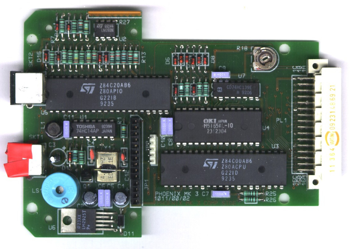
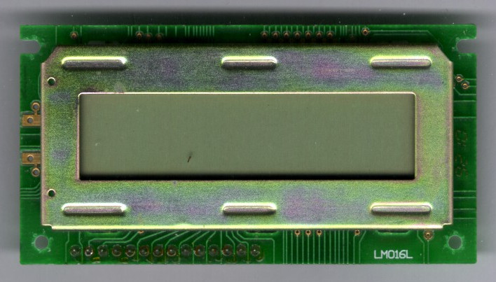
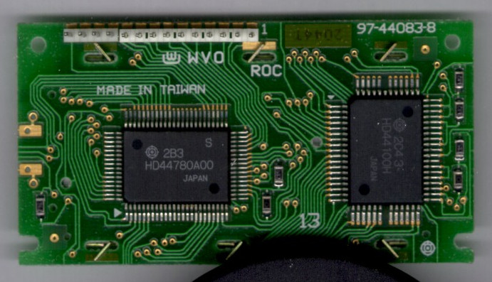
Externally, we can see that the ACR has a 2 x 16 character LCD display, a keypad with four keys (Up, Down, OK, and Esc), two mini DIN ports (one 6-pin and one 8-pin), and the 48-pin pod connector mentioned above. Looking inside, we find that it's a simple design based around a Zilog Z80 microprocessor (Z84C00), Z80 Parallel I/O controller (Z84C20), and an 8KB bank of SRAM (M5165AL-10). The PIO chip provides an interface to the serial port lines, the keypad inputs, and a piezo tweeter (which is made to beep when the user performs certain actions.) There is also a dual two-input demultiplexer (a Harris CD74HC139) to provide address decoding, and a couple other ICs to do input signal processing and line inverting. The LCD display is on a daughtercard module and controlled by a Hitachi HD44780.
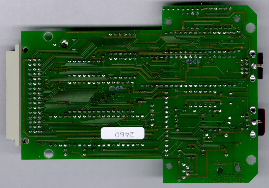
The silkscreening on the mainboard in my ACR unit identifies it as "Phoenix Mk 3, 1011/00/02".
The cable for the Rover MEMS SPi connects to the DIN port toward the right side of the handset; this port is identified as "SKT2" by the silkscreening on the mainboard, and it's the one without the red tape in the photo. Although the signal ground, transmit, and receive lines are all routed through this port for MEMS SPi communication, the firmware in the "Rover (1)" pod also asserts and de-asserts lines that are routed to the other DIN socket, SKT1. I'm not sure about the purpose of the SKT1 activity.
Tracing the CPU's address lines reveals the address map:
| Range | Device |
|---|---|
| Memory: $0000 - $7FFF | ROM (32KB) |
| Memory: $8000 - $9FFF | RAM (8KB) |
| I/O: $0000 - $0003 | PIO controller |
| I/O: $00C0 - $00C3 | LCD controller |
The 48-pin pod connector has three rows with sixteen pins each. Many of these pins are assigned directly to address, data, and chip-enable lines on the ROM (or flash) chip in the pod. The table below shows the pin assignments. I've tried to keep the table generic so as to apply to as many different pods as possible. Certain pods have additional pin assignments, so any blank entries in the table do not imply that a pin has no connection. CE, OE, and WE are 'chip enable', 'output enable', and 'write enable', respectively, although the last would only apply to pods that have writable storage, such as flash memory.
| Row | |||
|---|---|---|---|
| Pin number | A | B | C |
| 1 | GND | GND | GND |
| 2 | CE | D3 | D4 |
| 3 | D2 | D5 | |
| 4 | D1 | D6 | |
| 5 | D0 | D7 | |
| 6 | OE | A0 | |
| 7 | WE | A14 | A1 |
| 8 | A13 | A2 | |
| 9 | A12 | A3 | |
| 10 | A11 | A4 | |
| 11 | A10 | A5 | |
| 12 | A9 | A6 | |
| 13 | A8 | A7 | |
| 14 | GND | ||
| 15 | GND | ||
| 16 | Vcc |
Rover 1 pod (300565)
In the case of the "Rover 1" pod (part number 300565), the permanent storage is a UV-erasable EPROM (ST Micro M27C256B-12F1), which is covered with a sticker reading "1031-03-1 ISS1 / ROVER GB". There is also a small amount of circuitry specific to this pod, including a transistor switch for the TTL-level serial port output, as well as certain pins looped-back into the 48-pin mating connector.
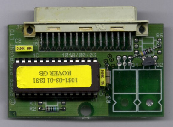

The 32KB ROM image in this pod contains about 12KB of code and data, with the remaining space filled by a repeating copyright message ("Design Copyright S.P Technology Group.", "Software Copyright G.J Clarkson 1993,1994.") There are some data tables and ASCII strings interspersed with executable code, but most of the strings are stored in a section between $224B and $309F that contains only data.
The code in the Rover 1 pod (and presumably other pods as well) performs a few self-tests on startup. It runs an integrity check on the RAM and computes a 16-bit checksum over the entire contents of the ROM. If the ROM checksum does not match the expected value, the display is changed to read "CHKSUM ERROR", together with both the expected and computed checksums. In this case, the code dead-ends in a JMP loop. Note that a bit error in the copyright-message filler text will cause a checksum error and prevent the ACR from functioning, even though no code or data would have been affected in this case.
The ACR does not have a dedicated hardware serial port controller, so the code manipulates and samples the serial port lines as a bit-bang interface. The desired baud rate is achieved through the use of tuned delay loops.
Rover 3 pod (30350800)
My Rover 3 pod is a later design than my Rover 1 pod. It contains programmable logic and flash memory, which probably allowed the manufacturer to more easily produce generic pods that can be programmed for any application. The Rover 3 pod still uses the same 48-pin main connector, but the design of the plastic housing is somewhat different because it was intended for use with the later ACR2 or ACR4. It will still work in the old-style ACR unit, although it sometimes requires the user to "scroll" a three- or four-line text message that cannot be shown in its entirety on the older two-line display.
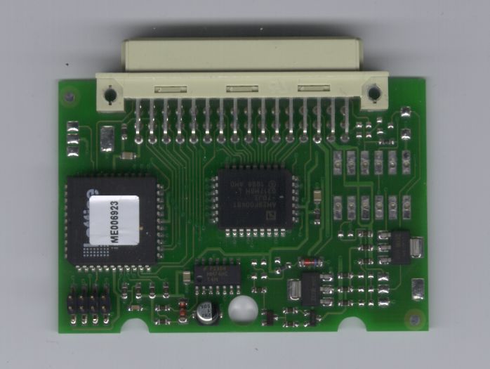
The permanent storage in this newer pod design is an AMD flash part, AM29F004BT-70JI. Also on the PCB is a Lattice ispLSI1016E-80LJ programmable logic device, and many of its I/O lines are tied to address and data lines on the flash. The PLD is in a PLCC44 package, and has a sticker on it that reads "ME006923", which likely identifies the revision of the image loaded to it. All of the parts are surface-mount, in contrast to the through-hole mounting used in the Rover 1 pod.
Another difference on the Rover 3 pod is the handling of the two highest address lines (A14 and A13): the main connector pins B7 and B8 are not connected directly to the A14 and A13 lines on the flash part. Instead, the connector pins are routed to two inputs on the PLD, which are 'I/O 7' and 'I/O 29'. By tracing the A14 and A13 flash pins, we can infer that a portion of the PLD logic uses this mapping:
| Function | PLD input | PLD output |
|---|---|---|
| A14 | I/O 7 (pin 22) | I/O 10 (pin 27) |
| A13 | I/O 29 (pin 8) | I/O 30 (pin 9) |
Finally, the card has a block of eight header pins. These provide a JTAG interface to program the Lattice PLD, using a variation of the PLD-JTAG pinout standard. Rather than being arranged in a single line, there are two columns of four pins each. Pin 1 is toward the nearest corner of the card, away from the 48-pin connector. The standard "nSRST" (system reset) JTAG pin is connected to the ispEN line on the PLD.